
Toshiba has begun shipping samples of its third-generation 3D NAND flash chip technology, which stacks 64 layers of flash cells and has 65% greater capacity than the previous generation technology, which used 48 layers.
“This increases memory capacity per silicon wafer and leads to a reduction of cost-per-bit,” Toshiba said in a statement.
 Toshiba
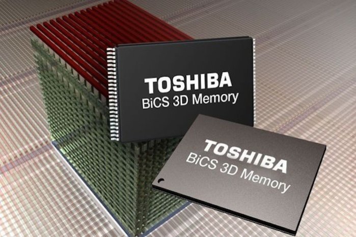
Based on a vertical stacking or 3D technology that Toshiba calls BiCS (Bit Cost Scaling), the company’s NAND flash memory stores three bits of data per transistor, meaning it’s a multi-level cell (MLC) flash chip. It can store 512Gbits (64GB) per chip.
To read this article in full or to leave a comment, please click here
Source: News Feed